Latest update: 2026-08-21
This guide illustrates how to generate and test a multi-core ESP SoC. This tutorial has many steps in common with the “How to: design a single-core SoC” tutorial, which is referenced by this guide multiple times. Make sure to complete the prerequisite tutorials before getting started with this one, as this guide builds on top of them without repeating content.
Intel/Altera development preview: the DE10-Pro SX instructions are not part of a released ESP version yet. Coming soon
- Target FPGA board
- SoC configuration
- Cache Configuration
- Debug link configuration
- FPGA prototyping
- FPGA prototyping with prebuilt material
Note: The users have access to prebuilt material to run the tutorial on an FPGA, without executing all the previous steps. See the ‘FPGA prototyping with prebuilt material’ section at the end of this guide.
Target FPGA board
Choose the working folder for your FPGA board. The SoC configuration steps are shared; synthesis, programming and payload loading use the vendor-specific targets described in the single-core SoC guide.
AMD/Xilinx example: VC707
cd <esp>/socs/xilinx-vc707-xc7vx485t
Intel/Altera example: Terasic DE10-Pro SX
cd <esp>/socs/terasic-de10-pro-sx
The DE10-Pro SX port is validated with Quartus Prime Pro 19.4. Its FPGA image must include the HPS bridge, so generate the matching HPS artifacts with Intel SoC EDS 19.1 before Quartus synthesis. See the board-specific section of the single-core guide for the exact commands.
SoC configuration
Open the ESP configuration GUI:
make esp-xconfig
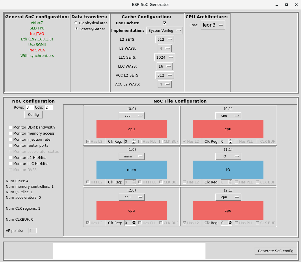
Select a 3x2 or 2x3 layout and set 4 processor tiles, 1 memory tile and 1
I/O tile, then save and close. The figure below shows the GUI with a possible
configuration for a quad-core ESP instance. ESP supports multi-core SoCs with
Leon3, Ariane and Ibex processor tiles. Make sure the ESP caches are enabled,
because they are mandatory for multi-core instances of ESP. To support
multi-core operation the ESP caches implement a directory-based MESI protocol
over the NoC.
Cache Configuration
The ESP Cache hierarchy is mandatory for a multi-core SoC. See the section “ESP Cache Hierarchy” from the “How to: design a single-core SoC” guide for more details. Use the RTL cache implementation for the Intel/Altera flow; the SystemC cache implementation requires HLS and is currently limited to AMD/Xilinx targets.
Debug link configuration
Follow the “Debug link configuration” instructions from the “How to: design a single-core SoC” guide.
FPGA prototyping
Follow the “FPGA prototyping” instructions from the “How to: design a
single-core SoC” guide. The only
difference is that before compiling Linux with the make linux command, you
should enable the Linux multi-core (Linux SMP) by setting a flag in the local
Makefile in the socs subfolder you’re working in.
SMP = 1
Note: The bare-metal “Hello ESP!” test executes on a single core. ESP provides bare-metal multicore programs, but they are outside the scope of this guide.
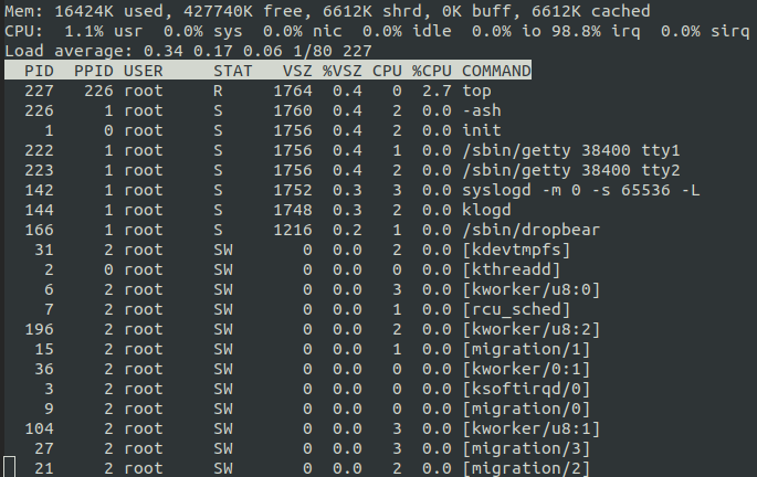
Once you login into Linux you can run top in the terminal to see that the
Linux processes are running on all four processor cores. See an example in the
image below:
FPGA prototyping with prebuilt material
Follow the “FPGA prototyping with prebuilt material” instructions from the “How to: design a single-core SoC” guide. The current prebuilt tutorial material targets AMD/Xilinx boards. Build the DE10-Pro SX image and HPS artifacts locally by following the Intel/Altera instructions instead.