Guide – How to: integrate ASIC memory macros into ESP
Latest update: 2023-05-31
This guide illustrates how to setup your ASIC project and how to integrate ASIC memory macros into ESP. At this moment, ESP memory integration supports only accelerators integrated into ESP using Stratus HLS. Refer to the guide How to: design an accelerator in SystemC (Cadence Stratus HLS) in the case you need a new accelerator integrated.
Note: Make sure to complete the prequisite tutorials before getting started with this one. This tutorial assumes that designers are familiar with the ESP infrastructure and know how to run basic make targets to create a simple instance of ESP, integrating just a single core.
0. Prerequisites
Memory integration requires at least the Verilog and the Liberty memory models/views from the technology.
1. Project setup and memory integration
Introduction
Memories are pervasive in ESP. They can be found in the IO tile for bootrom, in the CPU tile for L1 and L2 cache hierarchies, in the MEM tile for shared L3 cache hierarchy, in the accelerator tile for private local memory, and in the SLM tile for higher on-chip memory capacity. In this guide we will integrate ASIC memories into ESP, configure a SoC and perform RTL simulation stressing all tile types that have memories. This guide uses open-source memories generated by OpenRAM targeting Skywater 130 nm technology to exemplify the flow. The user, however, can follow this guide with the technology of your preference.
Project setup
The ESP FPGA flow uses the FPGA specific board under <esp>/socs as working directory for the SoC configuration, simulation, FPGA prototyping and validation. The ESP ASIC flow, instead, creates a directory structure outside the ESP repository. The directory structure has two main folders in addition to the ESP repository: technology folder and project folder. The technology folder has three directories: lib for memories and standard cells liberty files, mem_models for memory verilog models, and mem_wrappers for the memory wrappers. The project folder is the design working directory for the SoC configuration, RTL simulation and all ASIC flow downstream steps.
To create the ASIC directory structure execute the following steps:
# Create the main folder for your project and move the folder
mkdir project_x
cd project_x

# Clone ESP repository
git clone git@github.com:sld-columbia/esp.git

# Update the submodules
cd esp
git submodule update --init --recursive

# Move to asicgen folder
cd esp/tools/asicgen

# Edit the file asic_defs.sh with your project version and technology used
vim asic_defs.sh

DIRTECH_NAME="sky130"
PROJECT_NAME="projec_x_v1.0"

# Execute asic_dirstruct.sh script
./asic_dirstruct.sh
Once you have executed the steps above the project directory structure will be as follows:
project_x
├── project_x_v1.0
│   ├── Makefile
│   ├── ESP_ASIC_TOP.vhd     # ESP top level RTL
│   ├── chip_emu_top.vhd     # ESP top level wrapper to enable FGPA emulation
│   ├── esp_defconfig        # ESP SoC default configuration
│   ├── fpga_proxy_top.vhd   # FPGA proxy
│   ├── grlib_config.in
│   ├── grlib_defconfig
│   ├── pads_loc.vhd         # pad types (horizontal = 1 vertical = 0)
│   ├── systest.c            # main system simulation output
│   ├── testbench.vhd        # Top level testbench
│   └── top.vhd              # Top level composed by chip_emu_top and fpga_proxy_top
├── sky130
│   ├── lib                  # Technology folder for liberty files
│   ├── mem_models           # Technology folder for memory verilog models
│   └── mem_wrappers         # Memory verilog wrappers folder
└── esp
From now on, project_x_v1.0 is the working directory folder and the esp repository will be used ASIS.
Note: Do not create the directories manually, use the script for that!!!
ESP memory requirements
Although we work hard to make ESP as flexible as possible, ESP architecture has a few memory requirements listed bellow for each tile.
IO/AUX tile:
Two dual ports (1R1W) memories. The first of the size of 4096 addresses and 16 bits word length (4096x16). The second of the size of 256 addresses and 32 bits word length (256x32). They can be register files instead of memories.
One single port memory of 2048 addresses 8 bit word length (2048x8).
CPU tile:
One single port memory of 256 addresses and 64 bits word length (256x64) for Ariane L1 cache.
One single port memory of user choice address size and 64 bits word length for L2 line cache.
One single port memory of user choice address size and 24 bits word length for L2 mixed cache. This memory must support single bit write mask.
MEM tile:
One single port memory of user choice address size and 64 bits word length for L3 line cache.
One single port memory of user choice address size and 28 bits word length for L3 mixed cache. This memory must support single bit write mask.
One single port memory of user choice address size and 16 bits word length for L3 shared cache.
Note: The user address size for L2 and L3 caches must match. For instance, if a 256 address size is choosen for L2 line cache, the same address size has to be used for L2 mixed caches and all L3 level caches.
SLM tile:
One single port memory of user choice address size and 64 bits word length.
Accelerator tile:
The number of memory ports will depend on the accelerator used. The memory size, however, is flexible. ESP identifies all memories available for accelerators to automatically generate memory banks aiming to minimize memory area. According to the accelerator, some memory sizes will have a better performance and area efficiency. We suggest to have different memory sizes available for both types, dual and single ports. For instance: 256x8, 256x16, 256x32, 256x64, 512x32, 512x64, 1024x32, 1024x64.
Technology setup
Once you have generated all required memory macros for your target technology, you should copy/link the models to the respective folder in the project. In this guide we use soft links to avoid having multiple copies of the technology files.
Link the memory verilog models inside project_x/sky130/mem_models:
project_x/sky130/mem_models > ln -sf /tech/sky130/memories/sky130_sram_dp_256x32/sky130_sram_dp_256x32.v
project_x/sky130/mem_models > ln -sf /tech/sky130/memories/sky130_sram_dp_4096x16/sky130_sram_dp_4096x16.v
project_x/sky130/mem_models > ln -sf /tech/sky130/memories/sky130_sram_dp_512x32/sky130_sram_dp_512x32.v
project_x/sky130/mem_models > ln -sf /tech/sky130/memories/sky130_sram_sp_2048x8/sky130_sram_sp_2048x8.v
project_x/sky130/mem_models > ln -sf /tech/sky130/memories/sky130_sram_sp_256x64/sky130_sram_sp_256x64.v
project_x/sky130/mem_models > ln -sf /tech/sky130/memories/sky130_sram_sp_512x16/sky130_sram_sp_512x16.v
project_x/sky130/mem_models > ln -sf /tech/sky130/memories/sky130_sram_sp_512x64/sky130_sram_sp_512x64.v
Link the memory liberty models and the standard cell liberty model inside project_x/sky130/lib:
project_x/sky130/lib > ln -sf /tech/sky130/memories/sky130_sram_dp_256x32/sky130_sram_dp_256x32_TT_1p8V_25C.lib
project_x/sky130/lib > ln -sf /tech/sky130/memories/sky130_sram_dp_4096x16/sky130_sram_dp_4096x16_TT_1p8V_25C.lib
project_x/sky130/lib > ln -sf /tech/sky130/memories/sky130_sram_dp_512x32_1r1w/sky130_sram_sp_512x32_TT_1p8V_25C.lib
project_x/sky130/lib > ln -sf /tech/sky130/memories/sky130_sram_sp_2048x8/sky130_sram_sp_2048x8_TT_1p8V_25C.lib
project_x/sky130/lib > ln -sf /tech/sky130/memories/sky130_sram_sp_256x64/sky130_sram_sp_256x64_TT_1p8V_25C.lib
project_x/sky130/lib > ln -sf /tech/sky130/memories/sky130_sram_sp_512x16/sky130_sram_sp_512x16_TT_1p8V_25C.lib
project_x/sky130/lib > ln -sf /tech/sky130/memories/sky130_sram_sp_512x24/sky130_sram_sp_512x24_TT_1p8V_25C.lib
project_x/sky130/lib > ln -sf /tech/sky130/memories/sky130_sram_sp_512x28/sky130_sram_sp_512x28_TT_1p8V_25C.lib
project_x/sky130/lib > ln -sf /tech/sky130/memories/sky130_sram_sp_512x64/sky130_sram_sp_512x64_TT_1p8V_25C.lib
project_x/sky130/lib > ln -sf /tech/sky130/libraries/sky130_fd_sc_hs/latest/timing/sky130_fd_sc_hs__tt_025C_1v80.lib
Note 1: In this guide, we use a dual port 32 bits word length memory to replace the single port 28 bits word length memory for illustration purpose only.
Note 2: In this guide, we use single corner liberty to keep the guide short. We highly recommend, however, to link multiple liberty corners to enable multi-mode multi-corner timing analysis.
In the next section we will generate the memory wrapper skeletons and edit them to comply the ESP expected memory protocol with OpenRAM memory generated protocol.
ASIC memory list file
The memory wrapper skeletons are automatically generated based on the asic_memlist.txt specification file. The user needs to create this file in the project working directory (project_x/project_x_v1.0) compliant with the following syntax:
<type> <macro_name> <addr_size> <word_size> <area> <port_type>

Where:
<type> is the tile type (llc, l2, l1, slm, io, acc)
<macro_name> is the memory model module name
<addr_size> is the wrapper number of addresses
<word_size> is the wrapper word length
<area> is the memory model area
<port_type> is the number of memory model port (dual or single)
Bellow is an example of the asic_memlist.txt for the sky130 memories.
llc sky130_sram_sp_512x64 512 64 283536 single
llc sky130_sram_dp_512x32 512 28 294077 dual
llc sky130_sram_sp_512x16 512 16 110981 single
l2 sky130_sram_sp_512x64 512 64 283536 single
l2 sky130_sram_sp_512x24 512 24 128492 single
l1 sky130_sram_sp_256x64 256 64 175672 single
slm sky130_sram_sp_512x64 512 64 283536 single
io sky130_sram_dp_4096x16 4096 16 913452 dual
io sky130_sram_dp_256x32 256 32 197460 dual
io sky130_sram_sp_2048x8 2048 8 267554 single
acc sky130_sram_dp_256x32 256 32 197460 dual
acc sky130_sram_dp_512x32 512 32 294077 dual
acc sky130_sram_sp_512x64 512 64 283536 single
Note: Even though a dual port 32 bits word length memory is being used for the L2 mixed cache, the address size in the file remains 28 bits word length.
Once this file is ready, the execute the following command:
project_x/project_x_v1.0 > make mem_wrapper
A file called cache_def_mem_asic.v is generated in the working directory in addition to the memory wrapper skeletons in project_x/sky130/mem_wrapper.
In the next section we will edit the wrappers connecting the memory macro ports to the memory wrapper ports.
Memory wrappers edition
Move to the directory project_x/sky130/mem_wrapper. Under this deretory you will see the following files:
LLC_SRAM_SP_LINE_512x64.v
LLC_SRAM_SP_MIXED_512x28.v
LLC_SRAM_SP_SHARED_512x16.v
L2_SRAM_SP_LINE_512x64.v
L2_SRAM_SP_MIXED_512x24.v
L1_SRAM_SP.v
SLM_SRAM_SP_512x64.v
IO_DP_4096x16.v
IO_DP_256x32.v
IO_SP_2048x8.v
ACC_SRAM_DP_256x32.v
ACC_SRAM_DP_512x32.v
ACC_SRAM_SP_512x64.v
llc_lib.txt
l2_lib.txt
l1_lib.txt
slm_lib.txt
io_lib.txt
acc_lib.txt
The library text files (<mem>_lib.txt) gives the user the control of which memories to use according to the memory type. For instance, if there are several memories with different sizes available for accelerators but the user wants a specific memory for the FFT accelerator, it can just comment out all other memories in the acc_lib.txt file. This will force ESP to use only the uncommented memories for the FFT accelerator. By default, ESP selects the memory that gives the smaller area for each tile type.
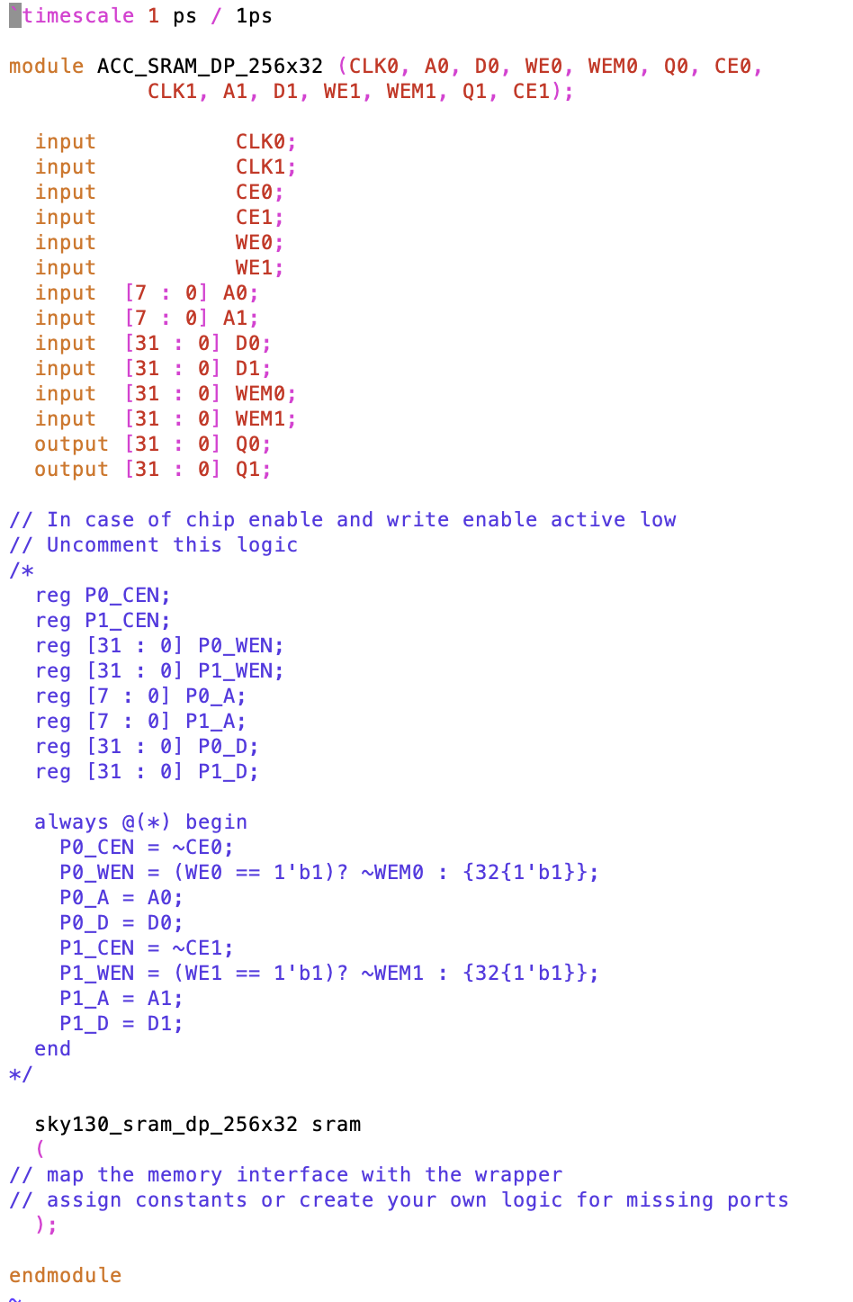
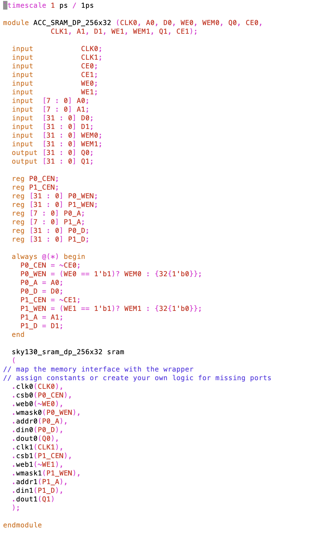
Each memory wrapper skeleton, shown bellow for the ACC_SRAM_DP_256x32, has the module name, its inputs and outputs compliant with ESP, the memory macro instantiation and a commented glue logic the user can adapt to match the ESP and the technology dependent memory macro protocols.

ESP expects single cycle memories compliant with the following protocol for single and dual port memories:
Single Port
| Port name | Diretion | Active | Description |
|---|---|---|---|
| CLK0 | Input | N/A | Clock port 0 |
| CE0 | Input | High | Chip enable port 0 |
| A0 | Input | N/A | Address port 0 |
| Q0 | Output | N/A | Output data port 0 |
| WE0 | Input | High | Write enable port 0 |
| WEM0 | Input | High | Write mask enable port 0 |
| D0 | Input | N/A | Input data port 0 |
Dual Port
| Port name | Direction | Active | Description |
|---|---|---|---|
| CLK0 | Input | N/A | Clock port 0 |
| CE0 | Input | High | Chip enable port 0 |
| A0 | Input | N/A | Address port 0 |
| Q0 | Output | N/A | Output data port 0 |
| CLK1 | Input | N/A | Clock port 1 |
| WE1 | Input | High | Write enable port 1 |
| WEM1 | Input | High | Write mask enable port 1 |
| A1 | Input | N/A | Address port 1 |
| D1 | Input | N/A | Input data port 1 |
We illustrate bellow the final edited wrapper for the memory generated by OpenRAM targeting Skywater 130 nm technology.

The user has the freedom to change all memory wrappers body to integrate its memory macros. This include instantiating multiple memory macros to compose a single wrapper. The module name, input and output ports, however, must remain the same.
In our example above for the LLC mixed cache, for instance, we are using only 28 bits of data and setting the remaining most significant bits to zero in the memory macro interface.
2. SoC generation
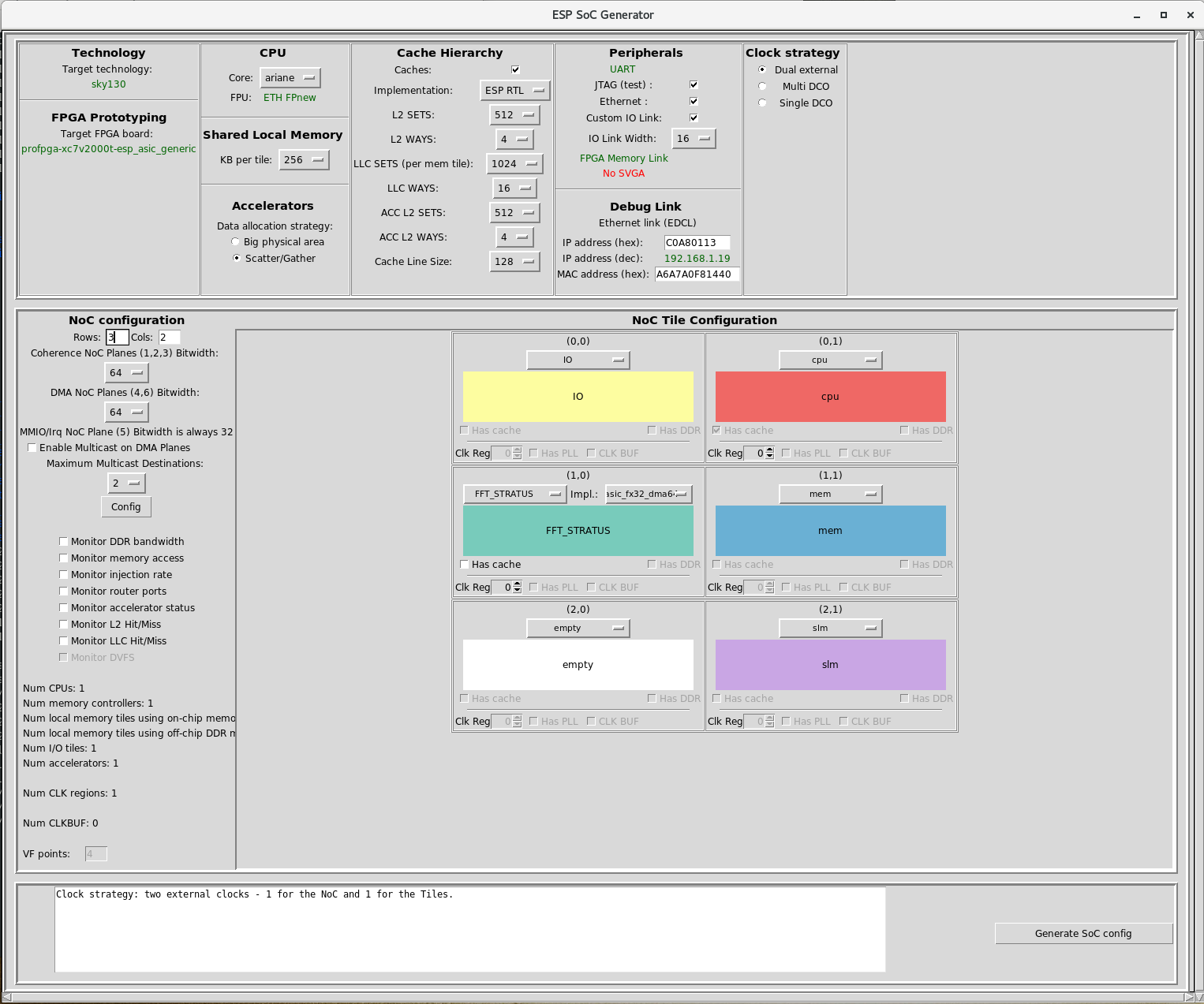
Once all technology models, liberty and verilog, are in the respective folders and the memory wrappers are completed, ESP SoC can be generated. In this tutorial, we are going to generate a SoC with the following tiles: IO, CPU (Ariane), MEM, SLM, and Acc (FFT).
The first step is to run High Level Synthesis of FFT to have a RTL based on the technology standard cell and memory timing models linked in project_x/sky130/lib. Then, we will generate the ESP SoC as usual. Finally we will simulate all tiles in our SoC.
HLS using ESP integrated FFT accelerator
To run HLS, execute the following command under project_x/project_x_v1.0:
project_x/projec_x_v1.0 > make fft_stratus-hls
ESP will run HLS for the already integrated FFT accelerator and will use the memory wrappers to generate the Private Local Memory (PLM) specified under project_x/esp/accelerators/stratus/fft_stratus/hw/memlist.txt.
The HLS results are saved in project_x/esp/tech/sky130/acc and project_x/esp/tech/sky130/memgen.
SoC configuration
The next step is to configure ESP SoC. Run the following command under project_x/project_x_v1.0 to call the ESP graphical interface:
project_x/project_x_v1.0 > make esp-xconfig
The composition of the SoC will have one IO tile, one MEM tile, one CPU (Ariane) tile, one SLM tile and one Acc (FFT) tile according to the image bellow.

Note we changed the size of the shared local memory to 64KB. The user can specify a range of sizes in the graphical interface and ESP will generate memory banks according to the SLM memory wrappers available in project_x/sky130/mem_wrappers/slm_lib.txt.
Once the SoC is configured, click in generate and close the window.
To generate the SLM banks with the size specified in the configuration, run the following step:
project_x/project_x_v1.0 > make mem_slmgen
The user can find the generated bank under project_x/esp/tech/sky130/memgen/slm_gen.
ESP is now ready for RTL simulation.
SoC RTL simulation: main system
The first simulation will confirm the IO tile, the CPU tile and the MEM tile are working properly. This simulation loads the bootloader into IO tile. Then, the IO tile starts the CPU tile which reads the bootram and executes read (instruction/data) and write (data) requests to the MEM tile. The MEM tile accesses the external memory according to the CPU tile requests. If the simulation succeed, a “Hello from ESP” message will show in the prompt.
Run the following command to execute the Modelsim simulation and confirm all memories were properly integrated.
project_x/project_x_v1.0 > make sim
Once all files were compiled and loaded, execute the simulation in Modelsim:
VSIM 1> run -all
Differently from FPGA, ASIC simulation does not have a simulation stop. Hence, type “ctrl c” to have Modelsim terminal back and close the tool.
SoC RTL simulation: accelerator
The second simulation will test the accelerator functionality in the SoC. This simulation invokes the accelerator baremetal program which directly accesses the MEM tile to read and write data. Three memory coherence protocols are tested: Non-coherent DMA, LLC-coherent DMA, and Coherent DMA.
Run the following commands to simulate the accelerator:
project_x/project_x_v1.0 > make fft_stratus-baremetal
project_x/project_x_v1.0 > TEST_PROGRAM=soft-build/ariane/baremetal/fft_stratus.exe make sim

VSIM 1> run -all
The prompt will state “PASS” for the three coherence modes. You can execute the same steps from previous section to close the tool.
SoC RTL simulation: shared local memory
Lastly, if your ESP configuration has the SLM tile, run the following command to confirm the memories integrated into SLM can be read and write properly:
project_x/project_x_v1.0 > make slm_rw_test-baremetal
project_x/project_x_v1.0 > TEST_PROGRAM=soft-build/ariane/baremetal/slm_rw_test.exe make sim
VSIM 1> run -all
The prompt message “Completed with 0 errors” confirms the test succeeded.