Guide – How to: integrate ASIC technology into ESP
Latest update: 2024-06-20
This guide illustrates how to setup your ASIC project and how to integrate ASIC technology into ESP. At the moment, ESP memory integration supports only accelerators designed with Stratus HLS (How to: design an accelerator in SystemC (Cadence Stratus HLS)) and SoCs that utilize the RISC-V Ariane core.
- 1. Project setup
- 2. Memory integration
- 3. Pad integration
- 4. SoC generation
- 5. Clocking strategy and DCO integration
Note: Make sure to complete the prequisite tutorials before getting started with this one. This tutorial assumes that designers are familiar with the ESP infrastructure and know how to run basic make targets to create a simple instance of ESP, integrating just a single core.
0. Prerequisites
ASIC technology integration requires at least the Verilog and the Liberty models/views for high level synthesis (HLS) and RTL simulation. In particular, this tutorial uses Skywater 130nm as an example technology. This requires the Skywater PDK and OpenRAM. For installation, please refer to the respective docmumentation of these projects.
1. Project setup
The ESP FPGA flow uses the FPGA-specific design folders under <esp>/socs as a
working directory for the SoC configuration, simulation, and FPGA prototyping.
The ESP ASIC flow, instead, creates a directory structure outside the ESP
repository. The directory structure has two main folders in addition to the ESP
repository: 1) a technology folder and 2) a project folder. The technology
folder has four directories: lib for memories, standard cells and gpio
liberty files; verilog for memories, standard cells and gpio verilog models;
mem_wrappers for the memory wrappers; and pad_wrappers for the IO wrappers.
The project folder is the working directory for SoC configuration, RTL
simulation, and all downstream steps of the ASIC flow.
To create the ASIC directory structure execute the following steps:
# Create the main folder for your project and move the folder
mkdir project_x
cd project_x

# Clone ESP repository
git clone git@github.com:sld-columbia/esp.git

# Interactively install submodules
cd esp
./utils/scripts/submodule_init.sh

# Move to asicgen folder
cd esp/tools/asicgen

# Edit the file asic_defs.sh with your project version and technology used
vim asic_defs.sh

DIRTECH_NAME="sky130"
PROJECT_NAME="projec_x_v1.0"

# Execute asic_dirstruct.sh script
./asic_dirstruct.sh
Once you have executed the steps above, the project’s directory structure will be as follows:
project_x
├── project_x_v1.0
│   ├── Makefile
│   ├── ESP_ASIC_TOP.vhd     # ESP top level RTL
│   ├── chip_emu_top.vhd     # ESP top level wrapper to enable FGPA emulation
│   ├── esp_defconfig        # ESP SoC default configuration
│   ├── fpga_proxy_top.vhd   # FPGA proxy
│   ├── grlib_config.in
│   ├── grlib_defconfig
│   ├── pads_loc.vhd         # default pad types (horizontal = 1 vertical = 0)
│   ├── vsim.tcl             # Modelsim script for simulation using DCO
│   ├── systest.c            # main system simulation output
│   ├── testbench.vhd        # Top level testbench
│   └── top.vhd              # Top level composed by chip_emu_top and fpga_proxy_top
├── sky130
│   ├── lib                  # Technology folder for liberty files
│   ├── verilog              # Technology folder for memory verilog models
│   ├── dco_wrappers         # DCO verilog wrappers folder
│   ├── mem_wrappers         # Memory verilog wrappers folder
│   │    └─ tb               # Memory verilog wrappers testbench folder
│   └── pad_wrappers         # IO verilog wrappers folder
└── esp
From now on, project_x_v1.0 is the working directory folder and the esp repository will be used ASIS.
Note: Do not create the directories manually, only use the provided scripts to do so!
2. Memory integration
ESP memory requirements
Although we work hard to make ESP as flexible as possible, the ESP architecture has a few memory requirements listed below for each tile.
IO/AUX tile:
Two dual port (1RW1R) memories are needed for the Ethernet MAC, when Ethernet
is enabled in the SoC. The first has a depth of 4096 words and 16-bit words
(4096x16). The second has a depth of 256 words and 32-bit words (256x32). They
can be register files instead of memories.
One single port memory with a depth of 2048 words and 8-bit words(2048x8).
CPU tile:
One single port memory with a depth of 256 words and 64-bit words (256x64)
for the Ariane L1 cache.
One single port memory with depth of user’s choice and 64-bit words for L2
cache lines.
One single port memory with depth of user’s choice and 24-bit words for L2
cache line metadata. This memory must support a bit-granularity write mask.
MEM tile:
One single port memory with depth of user’s choice and 64-bit words for LLC
cache lines.
One single port memory with depth of user’s choice and 28-bit words for the
LLC directory. This memory must support a bit granulariy write mask.
One single port memory with depth of user’s choice and 16-bit words for LLC
sharer’s lists.
Note: The chosen depth for L2 and LLC caches must match. For instance, if a depth of 256 is choosen for L2 cache lines, the same address size has to be used for L2 cache line metadata and all LLC memories.
SLM tile:
One single port memory with depth of user’s choice and 64-bit words.
Accelerator tile:
For the Stratus HLS design flow, ESP uses a custom tool (plmgen) to generate
the private local memory banks for the accelerator. plmgen can use both
single (1RW) and dual (2RW) port memories of any size. The tool will identify
all memories available to automatically generate memory banks with the
objective of minimizing area. According to the accelerator, some memory sizes
will have a better performance and area. We suggest to have different memory
sizes available for both types, dual and single ports. For instance: 256x8,
256x16, 256x32, 256x64, 512x32, 512x64, 1024x32, 1024x64.
Technology setup
Once you have generated all required memory macros for your target technology,
you should copy/link the models to the verilog folder in your project. In
this guide we use soft links to avoid having multiple copies of the technology
files.
Link the memory verilog models inside project_x/sky130/verilog:
project_x/sky130/verilog > ln -sf /tech/sky130/memories/sky130_sram_dp_256x32/sky130_sram_dp_256x32.v
project_x/sky130/verilog > ln -sf /tech/sky130/memories/sky130_sram_dp_4096x16/sky130_sram_dp_4096x16.v
project_x/sky130/verilog > ln -sf /tech/sky130/memories/sky130_sram_dp_512x32/sky130_sram_dp_512x32.v
project_x/sky130/verilog > ln -sf /tech/sky130/memories/sky130_sram_sp_2048x8/sky130_sram_sp_2048x8.v
project_x/sky130/verilog > ln -sf /tech/sky130/memories/sky130_sram_sp_256x64/sky130_sram_sp_256x64.v
project_x/sky130/verilog > ln -sf /tech/sky130/memories/sky130_sram_sp_512x16/sky130_sram_sp_512x16.v
project_x/sky130/verilog > ln -sf /tech/sky130/memories/sky130_sram_sp_512x64/sky130_sram_sp_512x64.v
project_x/sky130/verilog > ln -sf /tech/sky130/libraries/sky130_fd_sc_hs/latest/verilog/sky130_fd_sc_hs__tt_025C_1v80.v
project_x/sky130/verilog > ln -sf /tech/sky130/libraries/sky130_fd_io/latest/verilog/sky130_fd_io__top_gpiov2.behavioral.v
Link the memory liberty models and the standard cell liberty model inside project_x/sky130/lib:
project_x/sky130/lib > ln -sf /tech/sky130/memories/sky130_sram_dp_256x32/sky130_sram_dp_256x32_TT_1p8V_25C.lib
project_x/sky130/lib > ln -sf /tech/sky130/memories/sky130_sram_dp_4096x16/sky130_sram_dp_4096x16_TT_1p8V_25C.lib
project_x/sky130/lib > ln -sf /tech/sky130/memories/sky130_sram_dp_512x32_1r1w/sky130_sram_sp_512x32_TT_1p8V_25C.lib
project_x/sky130/lib > ln -sf /tech/sky130/memories/sky130_sram_sp_2048x8/sky130_sram_sp_2048x8_TT_1p8V_25C.lib
project_x/sky130/lib > ln -sf /tech/sky130/memories/sky130_sram_sp_256x64/sky130_sram_sp_256x64_TT_1p8V_25C.lib
project_x/sky130/lib > ln -sf /tech/sky130/memories/sky130_sram_sp_512x16/sky130_sram_sp_512x16_TT_1p8V_25C.lib
project_x/sky130/lib > ln -sf /tech/sky130/memories/sky130_sram_sp_512x24/sky130_sram_sp_512x24_TT_1p8V_25C.lib
project_x/sky130/lib > ln -sf /tech/sky130/memories/sky130_sram_sp_512x28/sky130_sram_sp_512x28_TT_1p8V_25C.lib
project_x/sky130/lib > ln -sf /tech/sky130/memories/sky130_sram_sp_512x64/sky130_sram_sp_512x64_TT_1p8V_25C.lib
project_x/sky130/lib > ln -sf /tech/sky130/libraries/sky130_fd_sc_hs/latest/timing/sky130_fd_sc_hs__tt_025C_1v80.lib
project_x/sky130/lib > ln -sf /tech/sky130/libraries/sky130_fd_io/latest/timing/sky130_fd_io__top_gpiov2_tt_tt_025C_1v80_3v30.lib
Note 1: In this guide, we use a dual port 32 bits word length memory to replace the single port 28 bits word length memory for illustration purpose only.
Note 2: In this guide, we use single corner liberty to keep the guide short. We highly recommend, however, to link multiple liberty corners to enable multi-mode multi-corner timing analysis.
In the next section, we will generate the memory wrapper skeletons and edit them to comply with the interfaces expected by ESP and used by the memory macros generated by OpenRAM.
ASIC memory list file
The memory wrapper skeletons are automatically generated based on the
asic_memlist.txt specification file. The user needs to create this file in
the project working directory (project_x/project_x_v1.0) with the following
syntax:
<type> <macro_name> <addr_size> <word_size> <area> <port_type>

Where:
<type> is the component type (llc, l2, l1, slm, io, acc)
<macro_name> is the memory model's module name
<addr_size> is the memory depth
<word_size> is the memory word size
<area> is the memory's area
<port_type> is the memory's number of ports (1RW, 2RW, 1RW1R)
The following is an example of the asic_memlist.txt for the sky130
memories.
llc sky130_sram_sp_512x64 512 64 283536 1rw
llc sky130_sram_dp_512x32 512 28 294077 2rw
llc sky130_sram_sp_512x16 512 16 110981 1rw
l2 sky130_sram_sp_512x64 512 64 283536 1rw
l2 sky130_sram_sp_512x24 512 24 128492 1rw
l1 sky130_sram_sp_256x64 256 64 175672 1rw
slm sky130_sram_sp_512x64 512 64 283536 1rw
io sky130_sram_dp_4096x16 4096 16 913452 1rw1r
io sky130_sram_dp_256x32 256 32 197460 1rw1r
io sky130_sram_sp_2048x8 2048 8 267554 1rw
acc sky130_sram_dp_256x32 256 32 197460 2rw
acc sky130_sram_dp_512x32 512 32 294077 2rw
acc sky130_sram_sp_512x64 512 64 283536 1rw
Note: Even though a dual-port, 32-bit word memory is being used for the L2 cache line metadata, the specified size is still 28 bits.
Once this file is ready, execute the following command:
project_x/project_x_v1.0 > make mem_wrapper
A file called cache_def_mem_asic.v is generated in the working directory in
addition to the memory wrapper skeletons in project_x/sky130/mem_wrappers.
In the next section we will edit the wrappers connecting the memory macro ports to the memory wrapper ports.
Memory wrappers editing
Move to the directory project_x/sky130/mem_wrappers. Under this directory you
will see the following files:
LLC_SRAM_SP_LINE_512x64.v
LLC_SRAM_SP_MIXED_512x28.v
LLC_SRAM_SP_SHARED_512x16.v
L2_SRAM_SP_LINE_512x64.v
L2_SRAM_SP_MIXED_512x24.v
L1_SRAM_SP.v
SLM_SRAM_SP_512x64.v
IO_DP_4096x16.v
IO_DP_256x32.v
IO_SP_2048x8.v
ACC_SRAM_DP_256x32.v
ACC_SRAM_DP_512x32.v
ACC_SRAM_SP_512x64.v
llc_lib.txt
l2_lib.txt
l1_lib.txt
slm_lib.txt
io_lib.txt
acc_lib.txt
The library text files (<mem>_lib.txt) give the user the control of which
memories to use according to the memory type. For instance, if there are
several memories with different sizes available for accelerators but the user
wants a specific memory for a particular accelerator, they only need to comment
out other memory types in acc_lib.txt. This will force plmgen to use only the
uncommented memories for that accelerator. By default, plmgen selects the
memory that gives the smaller area for each tile type.
Each memory wrapper skeleton, shown below for the ACC_SRAM_DP_256x32, has the module name, the inputs and outputs expected by ESP, the memory macro instantiation and commented glue logic the user can adapt to match the technology-dependent memory macro protocols.
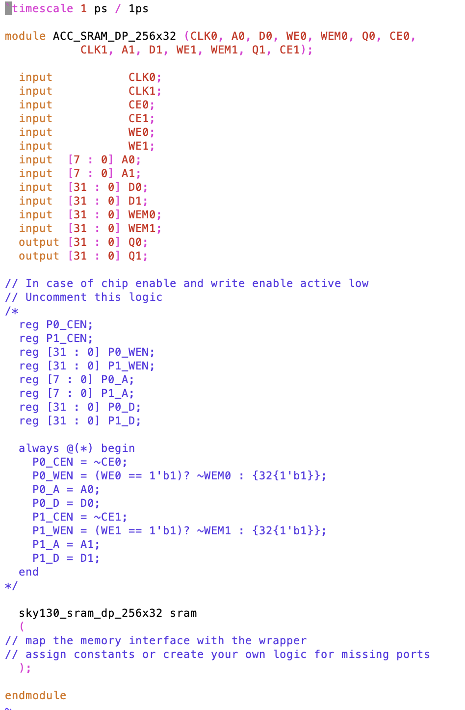
ESP expects single cycle memories compliant with the following protocol for single and dual port memories:
1RW Port
| Port name | Diretion | Active | Description |
|---|---|---|---|
| CLK0 | Input | N/A | Clock port 0 |
| CE0 | Input | High | Chip enable port 0 |
| A0 | Input | N/A | Address port 0 |
| D0 | Input | N/A | Input data port 0 |
| WE0 | Input | High | Write enable port 0 |
| WEM0 | Input | High | Write mask enable port 0 |
| Q0 | Output | N/A | Output data port 0 |
1RW1R Port
| Port name | Direction | Active | Description |
|---|---|---|---|
| CLK0 | Input | N/A | Clock port 0 |
| CE0 | Input | High | Chip enable port 0 |
| A0 | Input | N/A | Address port 0 |
| Q0 | Output | N/A | Output data port 0 |
| CLK1 | Input | N/A | Clock port 1 |
| CE1 | Input | High | Chip enable port 1 |
| A1 | Input | N/A | Address port 1 |
| D1 | Input | N/A | Input data port 1 |
| WE1 | Input | High | Write enable port 1 |
| WEM1 | Input | High | Write mask enable port 1 |
1RW1R Port
| Port name | Direction | Active | Description |
|---|---|---|---|
| CLK0 | Input | N/A | Clock port 0 |
| CE0 | Input | High | Chip enable port 0 |
| A0 | Input | N/A | Address port 0 |
| D0 | Input | N/A | Input data port 0 |
| WE0 | Input | High | Write enable port 0 |
| WEM0 | Input | High | Write mask enable port 0 |
| Q0 | Output | N/A | Output data port 0 |
| CLK1 | Input | N/A | Clock port 1 |
| CE1 | Input | High | Chip enable port 1 |
| A1 | Input | N/A | Address port 1 |
| D1 | Input | N/A | Input data port 1 |
| WE1 | Input | High | Write enable port 1 |
| WEM1 | Input | High | Write mask enable port 1 |
| Q1 | Output | N/A | Output data port 1 |
Below is the final edited wrapper for the memory generated by OpenRAM targeting Skywater 130 nm technology.
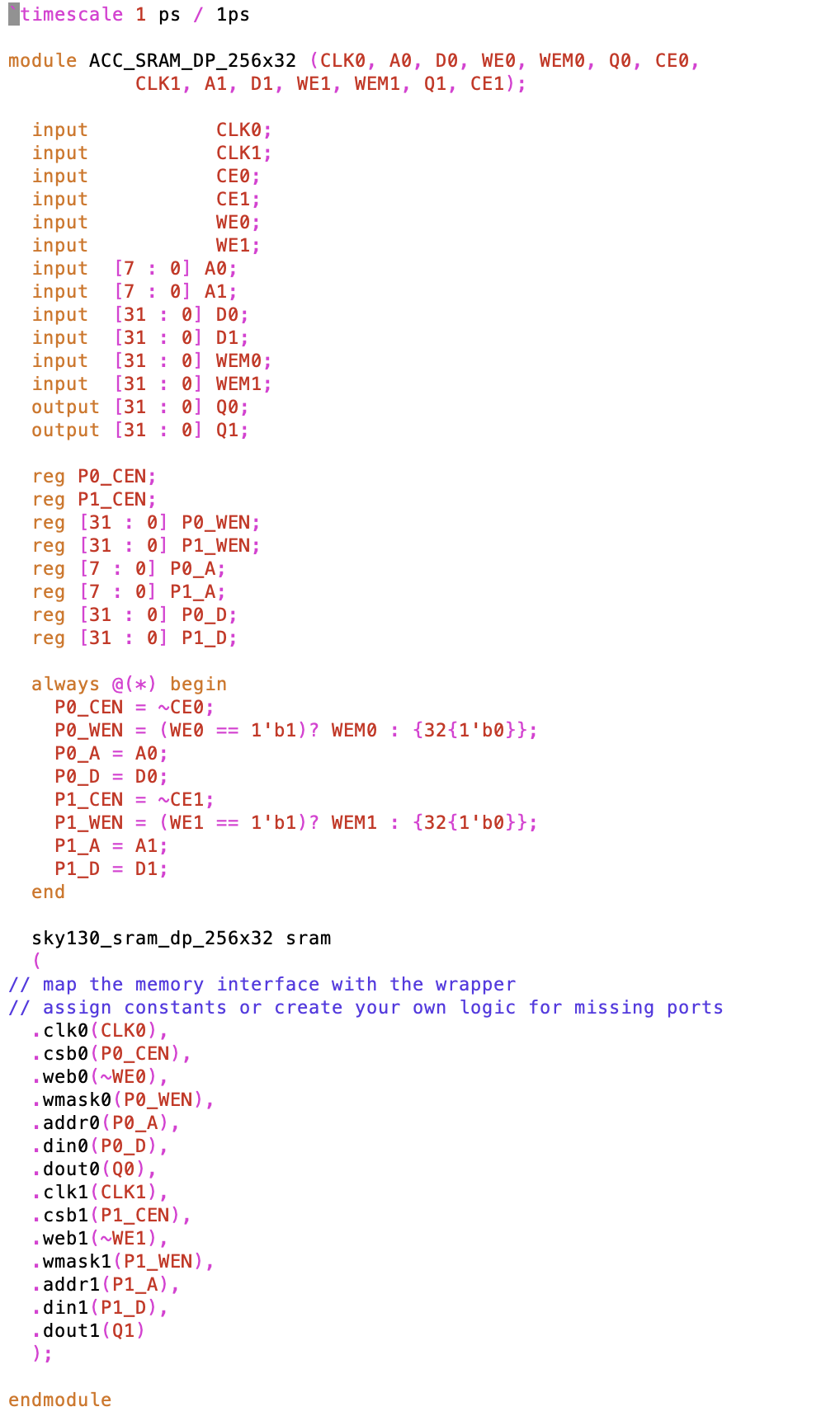
The user has the freedom to change the body of all memory wrappers to integrate the generated memory macros. This can include instantiating multiple memory macros inside a single wrapper to create the expected width and depth. The module name and input and output ports, however, must not be changed.
For example, when we use a 32-bit word macro for the LLC directory, which only requires 28-bit words, we set the 4 most-significant bits of the write data to zero and discard the 4 most-significant bits of read data.
Once the memory wrappers are completed they can be tested individually using
the testbenches automatically generated inside mem_wrappers/tb. These tests
ensure the memory wrappers are compliant with what ESP expects and can prevent
errors in full-system tests, which are lengthy to debug. The test succeeds when
it prints that zero errors occurred.
After all wrappers are successfully tested, the memory integration is completed. The next section will detail a similar process for the technology IO cells integration.
3. Pad integration
For each technology, there are different IO cells according to functionality and vendor. Therefore, supporting all interfaces that can exist for each cell type, vendor and technology is a challenging task. ESP supports the basic digital IO cell interfaces for inputs, outputs and bi-directional ports. ESP provides an additional 3-bit signal (CFG) for outputs that can be changed through a control and status register (CSR). This interface was added to configure slew rate and drive strength, but the user has freedom to use for other purposes.
The following sections details the IO cell integration process starting from the generation of pad wrapper skeletons and finishing with the population of these wrappers.
ASIC pad list files
The pad wrapper skeletons are automatically generated based on the
asic_padlist.txt specification file. The user needs to create this file in
the project working directory (project_x/project_x_v1.0) according to the
following syntax:
<direction> <macro_name> <location>

Where:
<direction> is the pad type (in, out, io)
<macro_name> is the pad model module name
<location> is the location of the pad (H for horizontal, V for vertical)
The location follows the illustration:
  _____________
 |\           /|
 | \   V(0)  / |
 |  \       /  |
 |   \     /   |
 |    \   /    |
 |     \ /     |
 | H(1) \ H(1) |
 |     / \     |
 |    /   \    |
 |   /     \   |
 |  /       \  |
 | /   V(0)  \ |
 |/___________\|
The following is an example of the asic_padlist.txt using the sky130 gpiov2 pads.
.
in sky130_fd_io__top_gpiov2 H
in sky130_fd_io__top_gpiov2 V
out sky130_fd_io__top_gpiov2 H
out sky130_fd_io__top_gpiov2 V
io sky130_fd_io__top_gpiov2 H
io sky130_fd_io__top_gpiov2 V
Note: All direction (in/out/io) and both types (H/V), are required. Since
sky130 gpiov2has only one inout model that can be configured in the three directions, we specified the same macro module in all six models.
Once the file is created, the user can generate the pad wrapper skeletons by running the following target:
project_x/project_x_v1.0 > make pad_wrapper
We provide a default VHDL file, pads_loc.vhd, that configures whether a H or V
pad is used for each IO signal. The default file accounts for one Memory tile
instantiation only. If the user would like to use more than one Memory tile or
would like to change the pad configuration (H or V), a customized file has to
be generated.
We provide a make target that generates the VHDL file based on a text file (pads_loc.txt) with the following format:
<signal> <index> <location>

where:
<signal> is the design port
<index> is the index of the port if it is an array
<location> is the location of the pad (0 for V and 1 for H)
Below is an example of the pads_loc.txt.
clk_div_acc0 0 0
clk_div_acc1 0 0
clk_div_cpu 0 0
dummy 0 0
erx_clk 0 0
erxd 0 0
erxd 1 0
erxd 2 0
erxd 3 0
erx_dv 0 0
etx_clk 0 0
ext_clk_acc0 0 0
ext_clk_acc1 0 0
ext_clk_cpu 0 0
fpga_clk_in 2 0
fpga_clk_in 3 0
...
To generate the customized pads_loc.vhd, run the target:
project_x/project_x_v1.0 > make pad_location
In the next section, we will edit the pad wrapper skeletons to be compliant with the ESP IO protocol.
Pad wrappers editing
Move to the directory project_x/sky130/pad_wrappers. Under this directory you will see the following files:
INPAD_H.v
INPAD_V.v
IOPAD_H.v
IOPAD_V.v
OUTPAD_V.v
OUTPAD_H.v
Each pad wrapper skeleton, shown below for the IOPAD_H.v, has the module
name, the inputs and outputs expected by ESP, and the pad macro instantiation.
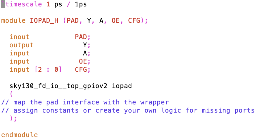
ESP expects the pads be compliant with following protocol for input, output and bi-directional pads:
Input pads
| Port name | Diretion | Active | Description |
|---|---|---|---|
| PAD | Inout | N/A | Pad inout port |
| Y | Output | N/A | Chip input pin |
Output pads
| Port name | Diretion | Active | Description |
|---|---|---|---|
| PAD | Inout | N/A | Pad inout port |
| A | Input | N/A | Chip output pin |
| CFG | Input | High | Pad configuration (3 bits) |
Bidirectional pads
| Port name | Diretion | Active | Description |
|---|---|---|---|
| PAD | Inout | N/A | Pad inout port |
| Y | Output | N/A | Chip input pin |
| A | Input | N/A | Chip output pin |
| OE | Input | High | Pad output enable pin |
| CFG | Input | High | Pad configuration (3 bits) |
The CFG is controlable by CSRs and can be used to configured the pad drive
strength, slew rate, or any other option available in the pad macro. Its
default value (on reset) is 011.
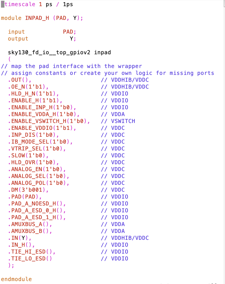
We illustrate below the final edited pad wrappers. Since the pads of location H and V have the same interface, we are illustrating only one of them.
Input pad
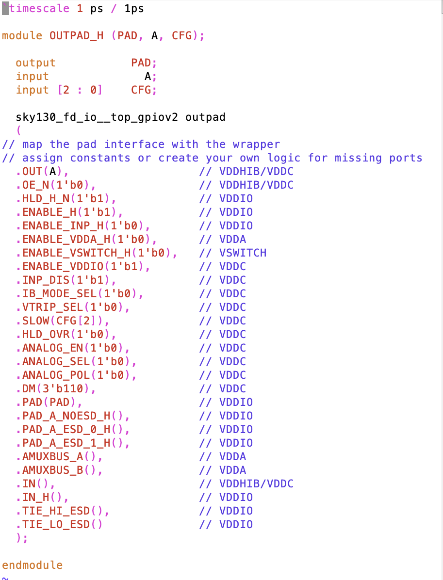
Output pad
Bi-directional pad
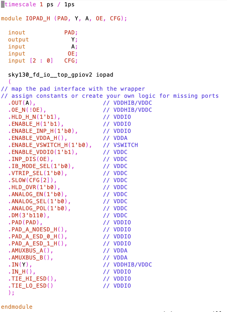
In the example above, some pad inputs are in a different power domain than the
core (VDDC and VDDHIB). HLD_H_N, ENABLE_H, and ENABLE_INP_H are in the
VDDIO power domain. ENABLE_VSWITCH_H is in the VSWITCH power domain. We tied
them to high or low for correct simulation of the verilog models. This is done
for simulation purposes only and, for logic synthesis and other downstream
physical design steps, these ports should be connected to the appropriate power
domain.
The user has the freedom to change the body of all pad wrappers to integrate the pad macros. The module name and input and output ports, however, must not be changed.
In these examples, we only used one bit of CFG to control the output slew
rate. The usage of all 3 bits will depend on the configurability of the pad and
the user’s design choices.
4. SoC generation
Once all technology models (liberty and verilog) are in the correct folders, and the memory and pad wrappers are completed, the ESP SoC can be generated. In this tutorial, we are going to generate a SoC with the following tiles: IO, CPU (Ariane), MEM, SLM, and Acc (FFT).
The first step is to run High Level Synthesis of the FFT accelerator to have
RTL based on the technology standard cell and memory timing models linked in
project_x/sky130/lib. Then, we will generate the ESP SoC as usual. Finally we
will simulate all tiles in our SoC.
HLS using ESP integrated FFT accelerator
To run HLS, execute the following command under project_x/project_x_v1.0:
project_x/projec_x_v1.0 > make fft_stratus-hls
ESP will run HLS for the already-integrated FFT accelerator and will use the
provided memory wrappers to generate the Private Local Memory (PLM) specified
under project_x/esp/accelerators/stratus/fft_stratus/hw/memlist.txt.
The outputs of HLS are saved in project_x/esp/tech/sky130/acc and
project_x/esp/tech/sky130/memgen.
SoC configuration
The next step is to configure the SoC. Run the following command under project_x/project_x_v1.0 to call the ESP graphical interface:
project_x/project_x_v1.0 > make esp-xconfig
Our target SoC contains one IO tile, one MEM tile, one CPU (Ariane) tile, one
SLM tile and one Accelerator (FFT) tile according to the image below.
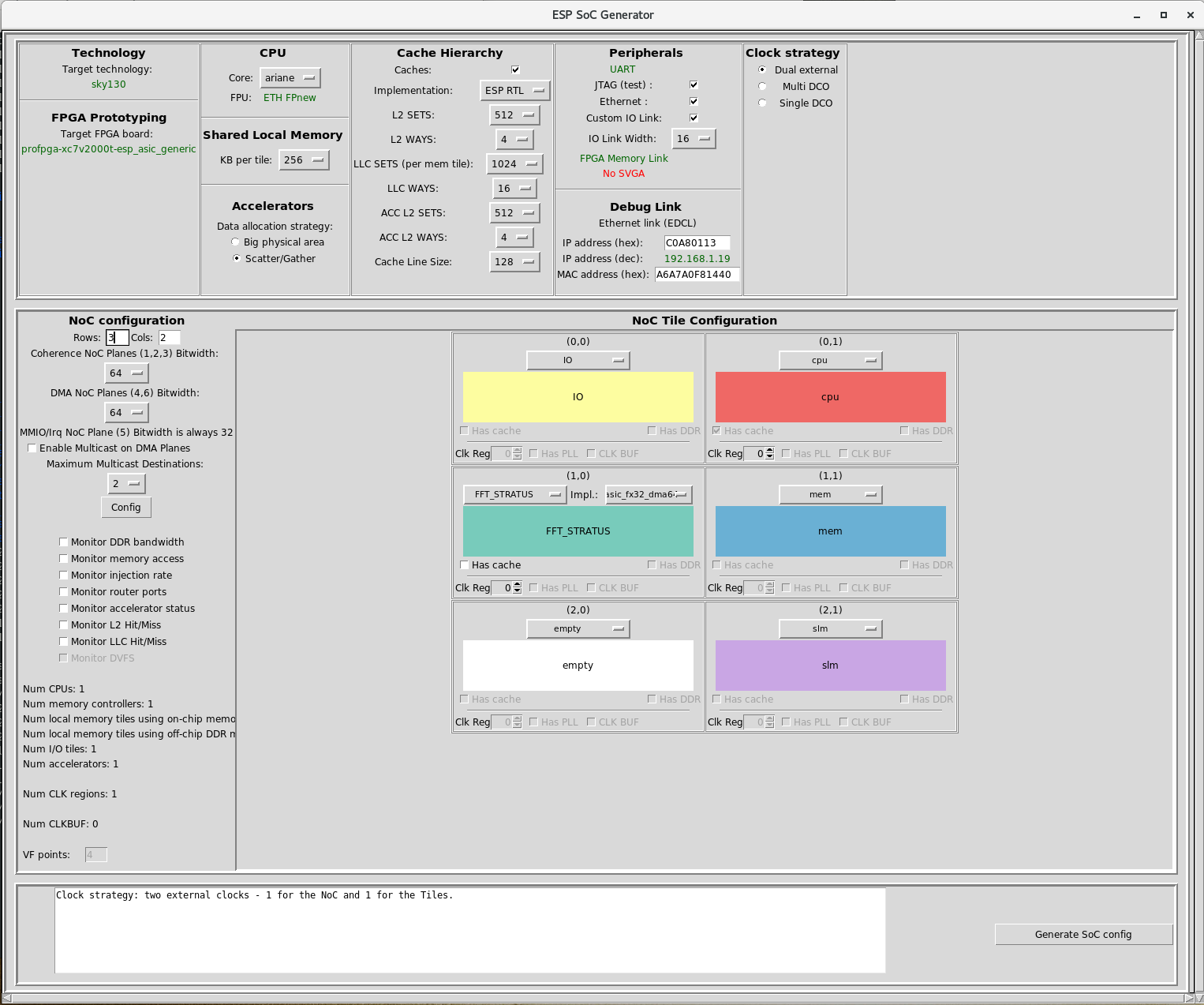
Here we set the size of the shared local memory tile to 64KB. The user can
select from a range of sizes in the graphical interface and ESP will generate
memory banks according to the SLM memory wrappers available in
project_x/sky130/mem_wrappers/slm_lib.txt.
Once the SoC is configured, click generate and close the window.
To generate the SLM banks with the size specified in the configuration, run the following step:
project_x/project_x_v1.0 > make mem_slmgen
The user can find the generated bank under project_x/esp/tech/sky130/memgen/slm_gen.
ESP is now ready for RTL simulation.
SoC RTL simulation: main system
The first simulation will confirm the IO tile, the CPU tile and the MEM tile are working properly. This simulation loads the bootloader into IO tile. Then, the IO tile starts the CPU tile which reads the bootram and executes read (instruction/data) and write (data) requests to the MEM tile. The MEM tile accesses the external memory according to the CPU tile requests. If the simulation succeed, a “Hello from ESP” message will show in the prompt.
Run the following command to execute the Modelsim simulation and confirm all memories were properly integrated.
project_x/project_x_v1.0 > make sim
Once all files were compiled and loaded, execute the simulation in Modelsim:
VSIM 1> run -all
SoC RTL simulation: accelerator
The second simulation will test the accelerator’s functionality in the SoC. This simulation invokes the accelerator baremetal program which accesses the MEM tile to read and write data. Three accelerator coherence modes are tested: Non-coherent DMA, LLC-coherent DMA, and Coherent DMA.
Run the following commands to simulate the accelerator:
project_x/project_x_v1.0 > make fft_stratus-baremetal
project_x/project_x_v1.0 > TEST_PROGRAM=soft-build/ariane/baremetal/fft_stratus.exe make sim

VSIM 1> run -all
The prompt will state “PASS” for the three coherence modes.
SoC RTL simulation: shared local memory
Lastly, if your SoC configuration has the SLM tile, run the following command to confirm the integrated memories can be read and written properly:
project_x/project_x_v1.0 > make slm_rw_test-baremetal
project_x/project_x_v1.0 > TEST_PROGRAM=soft-build/ariane/baremetal/slm_rw_test.exe make sim
VSIM 1> run -all
The prompt message “Completed with 0 errors” confirms the test succeeded.
5. Clocking strategy and DCO integration
There are several ways to provide the clock for the SoC. The simplest one is having a single clock for the whole system driven by an external (off-chip) oscillator. There are other factors in play, however, that can require more complex clocking schemes. For instance, SoCs that must operate in higher frequencies (GHz) need to generate the clock internally. In addition, large SoCs can have blocks operating in different frequencies, demanding a clock divider or separate clock generators.
This section details the clocking strategy options ESP supports and a Digital Clock Oscillator (DCO) specification and integration for high speed SoCs.
Clocking strategy
ESP supports three main clock strategy:
- Dual external: One clock source for the tiles and one for the NoC; both clocks are driven from external sources
- Multi DCO: Each tile has its own DCO. Similarly, the NoC has its own DCO located inside the IO tile
- Single DCO: There is only one DCO in the IO tile clocking the full SoC
In the ESP configuration GUI, the user can select one of these strategies. According to the selection, a message will appear in the white box below detailing the selected configuration.
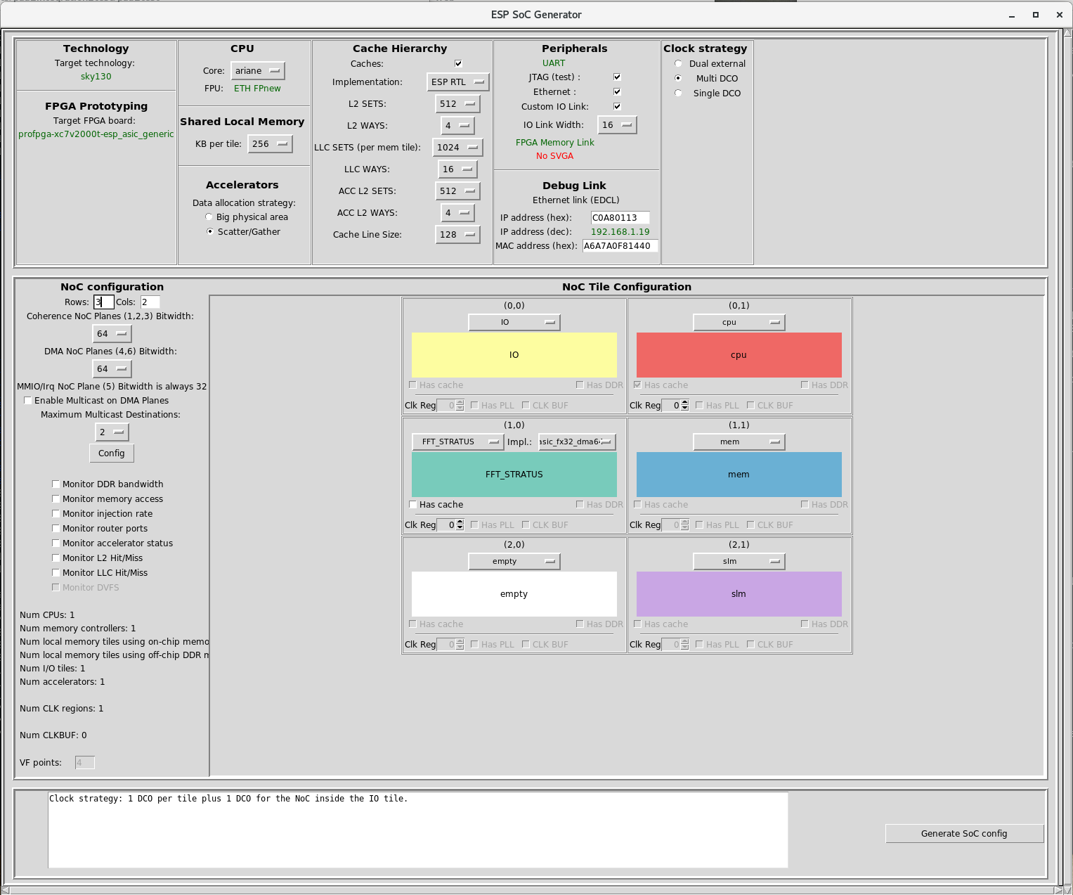
Except for the “Dual external” clocking strategy, the option we used for RTL simulation above, the user needs to provide a DCO mapped to the target technology compliant with ESP’s specification. The following sections details the DCO specfication and its integration to ESP for RTL simulation, logic synthesis, and place and route steps.
DCO specification
ESP provides 21 configuration bits from a CSR the user can leverage to
configure their own DCO block. For reference, we provide a technology
independent example of a DCO we used in our projects in
esp/rtl/techmap/inferred/. DCO_common.v has the primitives that need to be
mapped to the target technology. DCO.v instantiates the primitives in the DCO
top-level.
The following figure illustrates our reference DCO architecture:
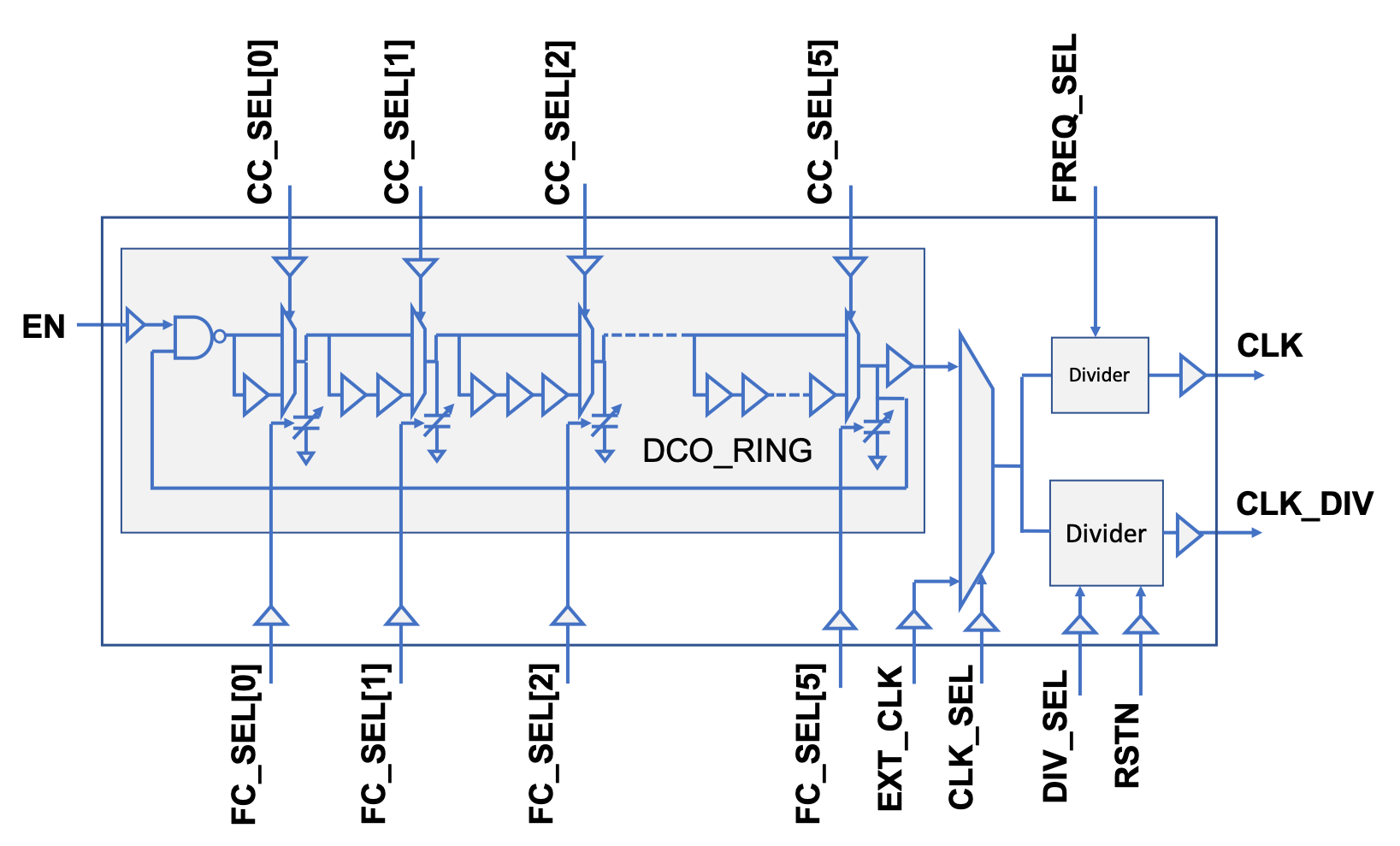
The following table details the reference DCO interface:
| Port name | Diretion | Active | Description |
|---|---|---|---|
| RSTN | Input | Low | Divider reset |
| EN | Input | High | Enable DCO oscillation |
| CC_SEL | Input | N/A | Coarse tune bits, the larger the value, the lower the CLK frequency (6 bits) |
| FC_SEL | Input | N/A | Fine tune bits, the larger the value, the lower the CLK frequency (6 bits) |
| EXT_CLK | Input | N/A | External clock source (Backup clock) |
| CLK_SEL | Input | N/A | Select clock: 0: DCO clock; 1: External clock |
| FREQ_SEL | Input | N/A | Divider for tile clock. 00: DCO clk, 01: DCO÷2, 11: DCO÷4 (2 bits) |
| DIV_SEL | Input | N/A | Divider ratio for test clock: 1: ÷2; 2: ÷4; 3: ÷8; …; 7: ÷128 (3 bits) |
| CLK | Output | N/A | High-speed clock for tile logic |
| CLK_DIV | Output | N/A | Divided clock. Routed off chip for testing |
Regardless of the chosen DCO architecture, Spice simulation of the technology-mapped DCO is highly recommended for frequency and jitter characterization in various corners.
DCO integration
ESP treats the DCO as a macro block, similarly to memories and standard cells. Therefore, it is expected that the following views are generated after place and route:
- DCO.v, DCO_common.v -> verilog used for RTL and netlist simulation
- DCO_tt.sdf -> standard delay formar (SDF) used for RTL and netlist simulation
- DCO.lib -> liberty view used for logic and physical synthesis
- DCO.lef -> layout exchange format (LEF) used for logic and physical synthesis
- DCO_pp.v -> verilog with power connections used for LVS
- DCO.gds -> used for DRC and LVS
Following our example for “project_x” using the technology skywater 130nm, the
DCO.v, DCO_common.v, and DCO_tt.sdf must be located at
project_x/sky130/dco_wrappers. The DCO.lib should be in
project_x/sky130/lib.
As long as the file and module names and the interface matches the reference provided and the views are located in the specified folders, the DCO is automatic integrated into ESP.
Since the current document targets RTL integration only, the remaining view locations will be detailed in the future.
SoC RTL simulation: main system using DCO clocking
To enable Modelsim to simulate the DCO with the annotated delays the user needs
to remove the comments inside project_x/project_x_v1.0/vsim.tcl to match the
following:
#echo "Restarting simulation with SDF annotation for DCO and delay line"
set sdf ""
set TECHLIB $::env(TECHLIB)
set ESP_ROOT $::env(ESP_ROOT)
set VSIMOPT $::env(VSIMOPT)
foreach inst [find instances -nodu -bydu DCO] {
    append sdf "-sdfmax "
    append sdf [string map {( [} [string map {) ]} $inst]]
    append sdf "=${ESP_ROOT}/rtl/techmap/${TECHLIB}/dco_wrappers/DCO_tt.sdf "
}
append sdf "-suppress 3438"
eval vsim $sdf $VSIMOPT
A similar script can be used for the XCelium simulator.
The RTL simulation targets are the same detailed in previous section. For “Hello from ESP” simulation, for instance, execute:
project_x/project_x_v1.0 > make sim